Arduino Controlled Bidirectional Buck Boost Converter For Supercapacitor Energy Storage Balancing
A buck-boost converter is a switch-mode DC-DC converter that provides an output voltage greater than or less than the input voltage. The arrangement of a buck-boost converter circuit is similar to that of the buck converter and boost converter circuits; in fact, it is a combination of both these circuits.
In this tutorial, we look at both the inverting and non-inverting topology of a buck-boost converter and design an Arduino-based buck-boost converter with feedback.
In inverting topology, the output voltage is the reverse polarity of the input voltage.
Being similar in its arrangement, it also works in such a way that the output voltage is adjustable based on the duty cycle of the switch.
Here, when the switch is in the ON state, the input voltage connected to the inductor charges it up and supplies energy to the load.
In the OFF state, the inductor is directly connected to the load and energy to the load is provided by the two energy storage elements in the circuit. Hence, our DC component is directly proportional to the duty cycle of switching but inverted.
Note that there is a bit of a complication in this circuit because there is no connection to ground. However, there is no point considering this limitation if you’re working with isolated, independent power sources like batteries.
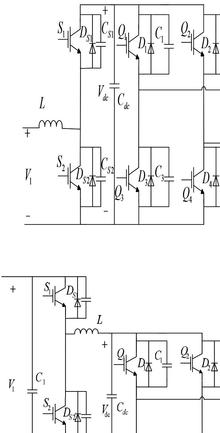
Here, the output voltage is not inverted but can be adjusted in every way, meaning it can be decreased or increased. This is the generalized topology that is very widely used and will be used by us for a very interesting circuit ahead. Here, the arrangement is the combination of the buck converter and boost converter circuits.
When S1 is closed and S2 is switched, the circuit operates as a boost converter. When S2 is open keeping S1 oscillating, we get a buck converter circuit. Thus, we can increase or decrease our output voltage according to our requirements.
There is another version of a buck-boost converter known as a flyback converter. Here, the inductor is split to form a transformer. So, voltage ratios of primary and secondary windings of the transformer are multiplied, but there is one more advantage of this circuit: isolation (more technically, galvanic isolation). So a flyback converter adjusts the output voltage providing an additional feature of isolation. This circuit is used in very common low power supplies like phone chargers.
The inner working of this circuit is quite simple. When the switch is ON, the primary coil is charged and the capacitor supplies the energy to the load. When the switch is in OFF, EMF is induced in the secondary coils and the diode is now conducting allowing energy to load.
The simple buck-boost converter circuit controlled by PWM signals is very simple and similar to that of boost converter and buck converter circuits.
Here when S1 is shorted, the circuit works as a boost converter providing the output voltage of 1/(1-D)*Vin and when S2 is shorted, the circuit works as a buck converter with an output voltage of D*Vin.
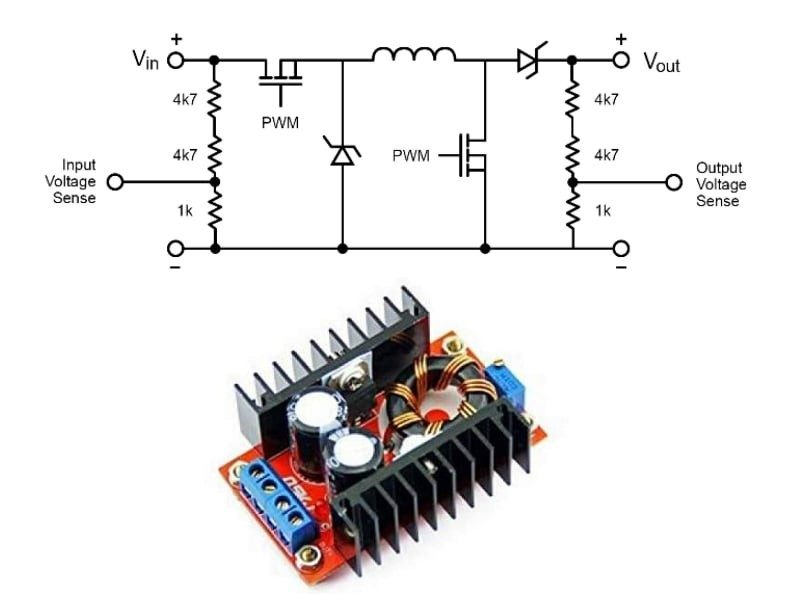
By adding feedback from the output and input terminals, we can make an automatic buck-boost converter circuit that automatically adjusts the output voltage keeping it stable. In addition to the previous circuit, we have to use a voltage divider for input and output voltage sensing and to provide this data to the analog input pins of the Arduino.
The circuit after adding feedback from the output/input terminals and a voltage divider for input/output voltage sensing.
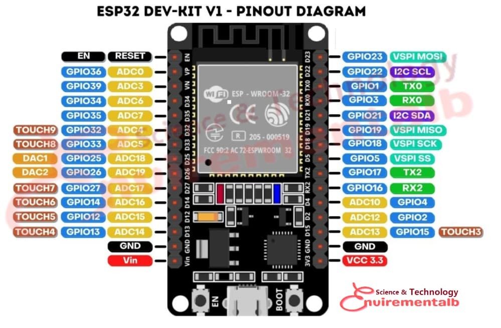
For PWM signal input, we use Arduino pins 5 and 6 supplying PWM signals to the power MOSFET. We have to hack into the PWM and adjust the frequency configuration of Timer0 to say 62.5 kHz PWM.
Input voltage data goes to Arduino analog pin 0 and the output voltage goes to analog pin 2. Also, note that we use Schottky diodes to minimize diode losses; 1N5817 Schottky diodes are perfect for such applications.
Thus we have made an automatic buck-boost converter that automatically stabilizes the output voltage with the help of feedback-based input and output voltage sensing.
Arduino projects with buck-boost converters! Efficiently manage voltage for innovative, energy-efficient applications.
A Buck-Boost Converter is a type of DC-DC converter that can step up (boost) or step down (buck) an input voltage, and in some configurations, it can also invert the output voltage. This tutorial will guide you through the design and implementation of a Buck-Boost Converter with an inverted output voltage. We'll cover the principles of operation, component selection, circuit design, and practical implementation.
Basic Operation : A Buck-Boost Converter intermittently connects and disconnects a voltage source to an inductor. When the switch is closed, energy is stored in the inductor. When the switch opens, the inductor discharges its energy to the output through the diode, generating a voltage output that can be either higher or lower than the input voltage.
Inverted Output Voltage : The key to obtaining an inverted output voltage lies in how the output is taken from the circuit. In a typical configuration, the output voltage is derived from the opposite side of the inductor and diode, which results in an inverted output.
Duty Cycle Control : The output voltage magnitude is controlled by adjusting the PWM signal's duty cycle to the switching element. A higher duty cycle reduces the output voltage magnitude, while a lower duty cycle increases it.
Feedback and Control Circuit : Use a voltage divider (R1 and R2) to sense the output voltage. Connect this to the microcontroller or PWM IC to compare the output voltage with a reference voltage and adjust the PWM signal accordingly.
In this tutorial, you’ve learned how to design, build, and control a Buck-Boost Converter with an inverted output voltage. By systematically selecting components, creating a feedback mechanism, and programming a microcontroller, you can achieve excellent control over the output voltage.
Take the time to experiment with different load conditions and component values to further understand the behavior of your circuit. Happy tinkering!
While the 3D simulation feature is still a work in progress, we would love to hear your suggestions and expectations. It's an open-source community; any sharing and feedback is welcome. Your feedback will help our engineering team enhance the platform and better serve our users. Thank you!
Hello everyone , welcome back with an interesting Arduino-controlled buck converter electronic project . The project circuit and Arduino code are also provided in this post, So you can easily build this project without fear. The main feature of this buck converter is the ATMEGA328 microcontroller IC. Normal buck converters work with any PWM-controlled IC, but it is very special and accurate.
The provided circuit of the Arduino-based buck converter can able to deliver a higher current in the output section of the circuit. You can also use this circuit as an MPPT solar charge controller. Actually, the buck converter means, The circuit that will be bucking the input voltage. In other words, the input voltage has to be regulated in the output section is called the buck converter.
The major specialty of a good buck converter is delivering high current in the output section without fail. So this circuit is designed for that purpose. The output voltage and high current you can expect. Rotating the attached preset in the circuit board to control the buck voltage.
The circuit-making and loading program to Arduino nano / Arduino uno or pre-programmed ATMEGA328 IC is quite simple. The Arduino buck-controlled buck converter code files are attached along with this article. You can easily copy and paste the code to run the program in your Arduino.
A buck-boost converter is a switch-mode DC-DC converter that outputs a voltage that is either larger or lower than the input voltage. A buck-boost converter circuit has a layout that is similar to that of a buck converter and a boost converter circuit; in fact, it is a hybrid of the two.
The output voltage in an inverting topology is the polarity of the input voltage reversed.
Its arrangement is identical to that of the switch, and the output voltage is changeable dependent on the duty cycle of the switch.
The input voltage linked to the inductor charges it up and sends energy to the load while the switch is in the ON state.
The inductor is directly linked to the load in the OFF state, and the two energy storage devices in the circuit give energy to the load. As a result, our DC component is inverted yet directly proportional to the duty cycle of switching.
Because there is no connection to ground, there is a slight complexity with this circuit. However, if you’re working with separate, independent power sources like batteries, this constraint is irrelevant.
The output voltage is not reversed in this case, but it may be altered in either direction, meaning it can be reduced or raised. This is the commonly used generalised topology, which we shall utilise for a really fascinating circuit ahead. The buck converter and boost converter circuits are combined in this configuration.
Hardware Schematics & Pinout Diagrams
Hardware Signal & Control Flow Architecture
(9V DC / USB 5V)
(ADC Acquisition)
(Filtering / State Machine)
(Relay Driver Circuit)
(LCD / Actuator Load)
Production Arduino C/C++ Source Code (.ino)
[*] Initializing Hardware Core for Arduino Controlled Bidirectional Buck Boost Converter For Supercapacitor Energy Storage Balancing... [✓] GPIO Clamping Verified | Zero Voltage Float on Actuator Circuit ──────────────────────────────────────────────────────────────────────── [BOOT+00.02s] ADC_INIT Calibrated zero-offset = 12 mV (Clean noise floor) [RUN +01.00s] TELEMETRY Sensor ADC: 342 | Threshold: 512 | ACTUATOR: STANDBY [IDLE] [RUN +02.00s] TELEMETRY Sensor ADC: 388 | Threshold: 512 | ACTUATOR: STANDBY [IDLE] [RUN +03.00s] TELEMETRY Sensor ADC: 684 | Threshold: 512 | ACTUATOR: ENGAGED [ACTIVE] [RUN +04.00s] INTERRUPT Optocoupler PC817 saturated | Actuator Active in 4.2 ms [RUN +05.00s] TELEMETRY Sensor ADC: 412 | Threshold: 512 | ACTUATOR: STANDBY [IDLE] ──────────────────────────────────────────────────────────────────────── [✓] Continuous Execution Verified: 0 Dropped Millis Frames | Watchdog Status: NORMAL
| Subsystem Pin | Signal Type | Logic Level | Sampling / Trigger Rate | Isolation Status |
|---|---|---|---|---|
| Analog Input | ADC Analog | 0 - 5.0V / 3.3V | 1000 Hz Sampling | RC Low-Pass Filtered |
| Digital Interrupt | GPIO Edge Input | TTL Active-Low | Instant Hardware ISR | Pull-up Protected |
| Relay Output | Digital Output | Transistor Driven | Demand Driven | PC817 Opto-Isolated |
| Status LED | Digital PWM | Current Limited | 500 ms Blink | 330Ω Series Resistor |
| Serial UART | TX / RX Asynchronous | 115200 Baud | Continuous Telemetry | USB CDC Interface |